|
| Function Test |
 >제품소개> Function Test >제품소개> Function Test |
|
|
|
| |
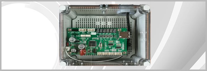
| AGV Main Board |
| |
 |
|
| |
|▶ 특징 |
| 1) |
AGV 확장 Port 사용으로 외부 PLC 제어 부분 대응 |
| 2) |
AGV Main BOARD에 오디오 칩 내장 / 안내,진행,경고 메시지 내장. |
| 3) |
통신 PORT(6) - Guide Sensor/PLC/ZiGbee/Barcode/Direct/확장 Port로 사용 중. |
| 4) |
RF모듈 장착하여 무선 RF 통신 지원. |
| 5) |
장착된 RF무선 Module 장비간 간섭 흡수 포함 (안테나 장착 시) 70M 사용 가능 . |
|
| |
|
| NO
|
ITEM
|
SPEC
|
DISC
|
|
1 |
Main Processor
(ARM or AVR ) |
System Main Control Process. |
|
Motor Control, Communication Control, PGA Control. |
2 |
FPGA Logic PLD
|
I/O Expander PLD. |
|
Motor Control Logic , I/O Control Logic. |
3 |
Motor Control Logic |
Motor Driver Control Interface. |
|
Motor Driver Signal Interface. |
4 |
Serial Interface |
RS-232 Buffer & Interface. |
|
5 |
Display
Set Part |
Main Board Display. |
|
Main Board Control Input KEY Unit. |
Main Board 각종 기능 설정 / 표시. |
6 |
Power Unit
|
Source 24Volt 공급 --> Switching Power. |
|
5 Volt / 3.3 Volt. |
7 |
Guide Sensor
Interface |
Guide Sensor Communication Interface. |
|
RS-422. |
|
|
| |
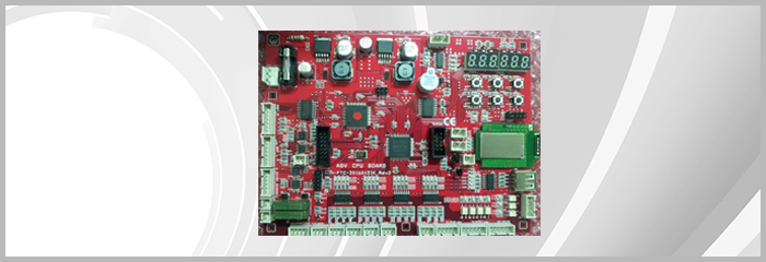
| RF Board - AGV |
| |
 |
|
| |
|▶ 특징 |
|
| |
|
| NO
|
PART
|
MODEL
|
SPEC
|
DISC
|
|
1 |
RF
Module |
PT2530HP1
|
RF
Chip : CC2530 + CC2591 |
|
Frequency
Band : 2394 – 2507 MHz |
Transmit
Power : < 18 dBm |
Receive
Sensitivity : -103 dBm |
Data
Rate : 250 Kbps |
Channel
: 16 |
Encryption
: AES |
Internal
Chip Ant |
2 |
Control MCU
|
ATMEGA1280A |
4 Serial Port ( 0
: RF, 1 : RF_TAG, 2 : AGV, 3 : SPARE ) |
|
3 |
Display
Set-Up |
SET-UP
|
FND
& KEY |
|
4 |
Power |
2596(150kHz) |
Input DC12V -- DC24V
|
|
5 |
EXT
Output DC |
|
DC5V
For RF Reader |
|
6 |
Input Port
|
PHOTO_ISO |
4 Channel ( DC24V
Source ) |
|
7 |
Output
Port |
PHOTO_ISO
|
4
Channel ( Open Collector Sink) |
|
|
|
| |
| RF BOARD - ACS |
| |
|
| |
|▶ 특징 |
|
| |
|
|
NO |
PART
|
MODEL
|
SPEC
|
DISC
|
|
1 |
RF
Module |
PT2530HP1
|
RF
Chip : CC2530 + CC2591 |
|
Frequency
Band : 2394 – 2507 MHz |
Transmit
Power : < 18 dBm |
Receive
Sensitivity : -103 dBm |
Data
Rate : 250 Kbps |
Channel
: 16 |
Encryption
: AES |
2 |
UTP
Module |
W5100 Module
|
Control Chip
W5100
TCP / IP / UTP |
|
3 |
Control
MCU |
ATMEGA1280A
|
4
Serial Port ( 0 : RF, 1 : UTP, 2 : SPARE,
3 : SPARE ) |
|
4 |
Display
Set-Up |
SET-UP |
FND & KEY
|
|
5 |
Power
|
2596(150KHZ)
|
Input
DC12V -- DC24V |
|
6 |
EXT
Output DC |
|
DC5V For RF
Reader |
|
7 |
Input
Port |
PHOTO_ISO
|
4
Channel ( DC24V Source ) |
|
8 |
Output
Port |
PHOTO_ISO |
4 Channel (
Open Collector Sink) |
|
9 |
Case
|
»상 투명 CASE |
SMPS
Include |
|
|
|
| |
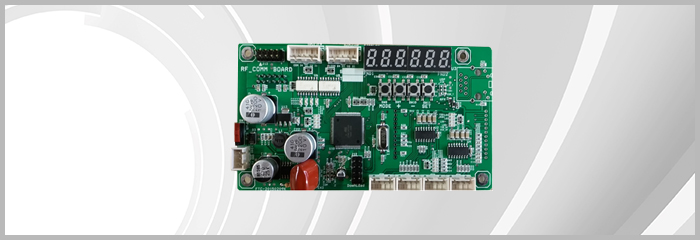
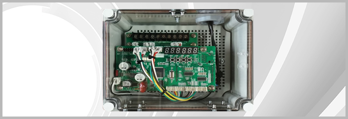
| RF BOARD - LINE |
| |
 |
|
| |
|▶ 특징 |
|
| |
|
|
NO |
PART
|
MODEL
|
SPEC
|
DISC
|
|
1 |
RF
Module |
PT2530HP1
|
RF
Chip : CC2530 + CC2591 |
|
Frequency
Band : 2394 – 2507 MHz |
Transmit
Power : < 18 dBm |
Receive
Sensitivity : -103 dBm |
Data
Rate : 250 Kbps |
Channel
: 16 |
Encryption
: AES |
Internal
Chip Ant |
2 |
Control
MCU |
ATMEGA1280A
|
4 Serial Port
( 0 : RF, 1 : UTP, 2: SPARE, 3 : SPARE ) |
|
3 |
Display
Set-Up |
SET-UP
|
FND
& KEY |
|
4 |
Power
|
2596(150kHz)
|
Input DC12V
-- DC24V |
|
5 |
EXT
Output DC |
|
DC5V
For Ext Power |
|
6 |
Input
Port |
PHOTO_ISO |
4 Channel (
DC24V Source ) |
|
7 |
Output
Port |
PHOTO_ISO
|
4
Channel ( Open Collector Sink )
|
|
8 |
Case
|
»상 투명 CASE |
SMPS Include
|
|
9 |
I/O
Terminal |
|
Terminal
Block Include |
|
|
|
| |
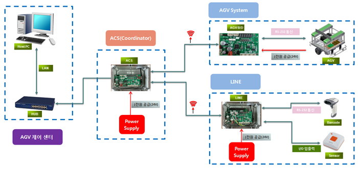
| AGV CONTROL SYSTEM –
BLOCK DIAGRAM |
| |
 |
|
| |
|
|